Publications
Chen, Jianglong; Leblanc, Valerie; Kang, Sung Hoon; Benning, Paul J.; Schut, David; Baldo, Marc A.; Schmidt, Martin A.; Bulović, Vladimir
High Definition Digital Fabrication of Active Organic Devices by Molecular Jet Printing Journal Article
In: Advanced Functional Materials, vol. 17, pp. 2722–2727, 2007.
@article{Chen2007,
title = {High Definition Digital Fabrication of Active Organic Devices by Molecular Jet Printing},
author = { Jianglong Chen and Valerie Leblanc and Sung Hoon Kang and Paul J. Benning and David Schut and Marc A. Baldo and Martin A. Schmidt and Vladimir Bulović},
url = {http://onlinelibrary.wiley.com/doi/10.1002/adfm.200601144/abstract},
year = {2007},
date = {2007-08-17},
journal = {Advanced Functional Materials},
volume = {17},
pages = {2722–2727},
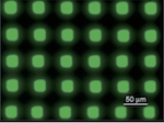
abstract = {We introduce a high resolution molecular jet (MoJet) printing technique for vacuum deposition of evaporated thin films and apply it to fabrication of 30 μm pixelated (800 ppi) molecular organic light emitting devices (OLEDs) based on aluminum tris(8-hydroxyquinoline) (Alq3) and fabrication of narrow channel (15 μm) organic field effect transistors (OFETs) with pentacene channel and silver contacts. Patterned printing of both organic and metal films is demonstrated, with the operating properties of MoJet-printed OLEDs and OFETs shown to be comparable to the performance of devices fabricated by conventional evaporative deposition through a metal stencil. We show that the MoJet printing technique is reconfigurable for digital fabrication of arbitrary patterns with multiple material sets and high print accuracy (of better than 5 μm), and scalable to fabrication on large area substrates. Analogous to the concept of “drop-on-demand” in Inkjet printing technology, MoJet printing is a “flux-on-demand” process and we show it capable of fabricating multi-layer stacked film structures, as needed for engineered organic devices.},
keywords = {},
pubstate = {published},
tppubtype = {article}
}
Leblanc, Valerie; Chen, Jianglong; Kang, Sung Hoon; Bulovic, Vladimir; Schmidt, Martin A.
Micromachined Printheads for the Evaporative Patterning of Organic Materials and Metals Journal Article
In: Journal of Microelectromechanical Systems, vol. 16, pp. 394 – 400 , 2007.
@article{Leblanc2007,
title = {Micromachined Printheads for the Evaporative Patterning of Organic Materials and Metals },
author = {Valerie Leblanc and Jianglong Chen and Sung Hoon Kang and Vladimir Bulovic and Martin A. Schmidt},
url = {http://ieeexplore.ieee.org/xpl/login.jsp?tp=&arnumber=4147590&url=http%3A%2F%2Fieeexplore.ieee.org%2Fiel5%2F84%2F4147571%2F04147590.pdf%3Farnumber%3D4147590},
year = {2007},
date = {2007-04-10},
journal = {Journal of Microelectromechanical Systems},
volume = {16},
pages = {394 - 400 },
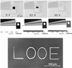
abstract = {This paper describes the design, fabrication, and testing of electrostatically actuated microshutters used as active shadow masks to pattern evaporated materials. The fabricated microshutters can obstruct a 25-mum-wide aperture at an actuation voltage of 90 V, with a resonant frequency of 4 kHz due to a 400-mum-long actuator. The microshutters integrated with an x-y-z manipulator were used to print patterns of organic material and metal on glass substrates in vacuum with a pixel size of 25 mum. The maximum resolution achievable with this setup is 800 dpi, and we printed active organic light-emitting device arrays of 400 dpi resolution. This printing scheme could enable the patterning of large-area organic optoelectronic devices on diverse substrates.},
keywords = {},
pubstate = {published},
tppubtype = {article}
}
Kang, Sung Hoon; Crisp, Todd; Kymissis, Ioannis; Bulović, Vladimir
Memory Effect from Charge Trapping in Layered Organic Structures Journal Article
In: Applied Physics Letters, vol. 85, pp. 4666-4668, 2004.
@article{Kang2004,
title = {Memory Effect from Charge Trapping in Layered Organic Structures},
author = {Sung Hoon Kang and Todd Crisp and Ioannis Kymissis and Vladimir Bulović},
url = {http://scitation.aip.org/content/aip/journal/apl/85/20/10.1063/1.1819991},
year = {2004},
date = {2004-11-15},
journal = {Applied Physics Letters},
volume = {85},
pages = {4666-4668},
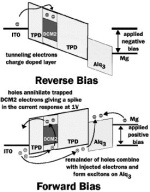
abstract = {We demonstrate organic light emitting devices(OLEDs) with a charge trap layer that show memory behavior. These OLEDs demonstrate that organic heterojunction structures can controllably trap and release electronic charges. The trap layer is either 5-nm-thick clustered silver islands, or a 10-nm-thick organic laser dye DCM2 ([2-methyl-6-[2-(2,3,6,7-tetrahydro-1H,5H-benzo[i,j]quinolizin-9-yl)-ethenyl]-4H-pyran-4-ylidene] propane-dinitrile) doped into TPD (N,N′-diphenyl-N,N′-bis(3-methylphenyl)-1,1′-biphenyl-4,4′-diamine). Predictions of the energy band structure indicate that both DCM2 sites and the metal islands can trap charge, consistent with the measured current–voltage characteristics. Trap sites are charged by applying reverse bias over the OLEDs. For devices with DCM2 traps we observe quenching of DCM2 photoluminescence upon charging, which allows us to quantify the charged trap density as approximately 10% of the trap sites or 10^18cm^−3. From time resolved measurements we observe that the charge retention time exceeds 2h.},
keywords = {},
pubstate = {published},
tppubtype = {article}
}
Note: Send e-mail to Prof. Kang at shkang@jhu.edu if you need a pdf file of the papers below.
2007
Chen, Jianglong; Leblanc, Valerie; Kang, Sung Hoon; Benning, Paul J.; Schut, David; Baldo, Marc A.; Schmidt, Martin A.; Bulović, Vladimir
High Definition Digital Fabrication of Active Organic Devices by Molecular Jet Printing Journal Article
In: Advanced Functional Materials, vol. 17, pp. 2722–2727, 2007.
Abstract | Links | BibTeX | Tags: Active, Device, Digital, Fabrication, High Definition, Molecular Jet, Organic, Printing
@article{Chen2007,

title = {High Definition Digital Fabrication of Active Organic Devices by Molecular Jet Printing},

author = { Jianglong Chen and Valerie Leblanc and Sung Hoon Kang and Paul  J. Benning and David Schut and Marc  A. Baldo and Martin  A. Schmidt and Vladimir Bulović},

url = {http://onlinelibrary.wiley.com/doi/10.1002/adfm.200601144/abstract},

year  = {2007},

date = {2007-08-17},

journal = {Advanced Functional Materials},

volume = {17},

pages = {2722–2727},

abstract = {We introduce a high resolution molecular jet (MoJet) printing technique for vacuum deposition of evaporated thin films and apply it to fabrication of 30 μm pixelated (800 ppi) molecular organic light emitting devices (OLEDs) based on aluminum tris(8-hydroxyquinoline) (Alq3) and fabrication of narrow channel (15 μm) organic field effect transistors (OFETs) with pentacene channel and silver contacts. Patterned printing of both organic and metal films is demonstrated, with the operating properties of MoJet-printed OLEDs and OFETs shown to be comparable to the performance of devices fabricated by conventional evaporative deposition through a metal stencil. We show that the MoJet printing technique is reconfigurable for digital fabrication of arbitrary patterns with multiple material sets and high print accuracy (of better than 5 μm), and scalable to fabrication on large area substrates. Analogous to the concept of “drop-on-demand” in Inkjet printing technology, MoJet printing is a “flux-on-demand” process and we show it capable of fabricating multi-layer stacked film structures, as needed for engineered organic devices.},

keywords = {Active, Device, Digital, Fabrication, High Definition, Molecular Jet, Organic, Printing},

pubstate = {published},

tppubtype = {article}

}
Leblanc, Valerie; Chen, Jianglong; Kang, Sung Hoon; Bulovic, Vladimir; Schmidt, Martin A.
Micromachined Printheads for the Evaporative Patterning of Organic Materials and Metals Journal Article
In: Journal of Microelectromechanical Systems, vol. 16, pp. 394 – 400 , 2007.
Abstract | Links | BibTeX | Tags: Evaporation, Fabrication, Metal, Organic, Patterning, Printing
@article{Leblanc2007,

title = {Micromachined Printheads for the Evaporative Patterning of Organic Materials and Metals },

author = {Valerie Leblanc and Jianglong Chen and Sung Hoon Kang and Vladimir Bulovic and Martin A. Schmidt},

url = {http://ieeexplore.ieee.org/xpl/login.jsp?tp=&arnumber=4147590&url=http%3A%2F%2Fieeexplore.ieee.org%2Fiel5%2F84%2F4147571%2F04147590.pdf%3Farnumber%3D4147590},

year  = {2007},

date = {2007-04-10},

journal = {Journal of Microelectromechanical Systems},

volume = {16},

pages = {394 - 400 },

abstract = {This paper describes the design, fabrication, and testing of electrostatically actuated microshutters used as active shadow masks to pattern evaporated materials. The fabricated microshutters can obstruct a 25-mum-wide aperture at an actuation voltage of 90 V, with a resonant frequency of 4 kHz due to a 400-mum-long actuator. The microshutters integrated with an x-y-z manipulator were used to print patterns of organic material and metal on glass substrates in vacuum with a pixel size of 25 mum. The maximum resolution achievable with this setup is 800 dpi, and we printed active organic light-emitting device arrays of 400 dpi resolution. This printing scheme could enable the patterning of large-area organic optoelectronic devices on diverse substrates.},

keywords = {Evaporation, Fabrication, Metal, Organic, Patterning, Printing},

pubstate = {published},

tppubtype = {article}

}
2004
Kang, Sung Hoon; Crisp, Todd; Kymissis, Ioannis; Bulović, Vladimir
Memory Effect from Charge Trapping in Layered Organic Structures Journal Article
In: Applied Physics Letters, vol. 85, pp. 4666-4668, 2004.
Abstract | Links | BibTeX | Tags: Charge Trap, Device, Layer, Memory, Organic
@article{Kang2004,

title = {Memory Effect from Charge Trapping in Layered Organic Structures},

author = {Sung Hoon Kang and Todd Crisp and Ioannis Kymissis and Vladimir Bulović},

url = {http://scitation.aip.org/content/aip/journal/apl/85/20/10.1063/1.1819991},

year  = {2004},

date = {2004-11-15},

journal = {Applied Physics Letters},

volume = {85},

pages = {4666-4668},

abstract = {We demonstrate organic light emitting devices(OLEDs) with a charge trap layer that show memory behavior. These OLEDs demonstrate that organic heterojunction structures can controllably trap and release electronic charges. The trap layer is either 5-nm-thick clustered silver islands, or a 10-nm-thick organic laser dye DCM2 ([2-methyl-6-[2-(2,3,6,7-tetrahydro-1H,5H-benzo[i,j]quinolizin-9-yl)-ethenyl]-4H-pyran-4-ylidene] propane-dinitrile) doped into TPD (N,N′-diphenyl-N,N′-bis(3-methylphenyl)-1,1′-biphenyl-4,4′-diamine). Predictions of the energy band structure indicate that both DCM2 sites and the metal islands can trap charge, consistent with the measured current–voltage characteristics. Trap sites are charged by applying reverse bias over the OLEDs. For devices with DCM2 traps we observe quenching of DCM2 photoluminescence upon charging, which allows us to quantify the charged trap density as approximately 10% of the trap sites or 10^18cm^−3. From time resolved measurements we observe that the charge retention time exceeds 2h.},

keywords = {Charge Trap, Device, Layer, Memory, Organic},

pubstate = {published},

tppubtype = {article}

}