Publications
Kang, Sung Hoon; Michael D. Dickey, Guest Editors
Patterning via self-organization and self-folding: Beyond conventional lithography Journal Article
In: MRS Bulletin, vol. 41, no. 2, pp. 93-96, 2016, (co-Guest Editor of the issue).
@article{Kang2016,

title = {Patterning via self-organization and self-folding: Beyond conventional lithography },

author = {Sung Hoon Kang and Michael D. Dickey, Guest Editors},

editor = {Sung Hoon Kang and Michael D. Dickey},

url = {http://journals.cambridge.org/download.php?file=%2FMRS%2FMRS41_02%2FS0883769416000038a.pdf&code=ffd6509119daa4a591802b67ab63f032},

doi = {10.1557/mrs.2016.3 },

year  = {2016},

date = {2016-02-01},

journal = {MRS Bulletin},

volume = {41},

number = {2},

pages = {93-96},

abstract = {Conventional photolithography is an effective patterning technique that has enabled modern

electronics and advanced micro- and nanoscale devices. However, it has limitations, including

high cost, limited resolution, and poor compatibility with unconventional materials that may be

soft, nonplanar, or difficult to process. There is active research ongoing to develop unconventional

patterning methods such as self-organization and self-folding. Self-organization harnesses

various driving forces to produce patterns without external intervention and includes

methods such as self-assembly of block copolymers, capillary-driven assembly of micro-/

nanoscale structures, and thin-fi lm instabilities. Self-folding (origami)—and its cousin,

kirigami—harnesses patterning and materials strategies to convert planar substrates into

three-dimensional shapes in response to external stimuli. These multidisciplinary approaches

open many engineering opportunities by providing new and versatile material functionalities.

This article overviews the field and the topics covered in the articles in this issue of  MRS Bulletin, highlighting recent progress in patterning approaches based on self-organization and self-folding. },

note = {co-Guest Editor of the issue},

keywords = {},

pubstate = {published},

tppubtype = {article}

}
electronics and advanced micro- and nanoscale devices. However, it has limitations, including
high cost, limited resolution, and poor compatibility with unconventional materials that may be
soft, nonplanar, or difficult to process. There is active research ongoing to develop unconventional
patterning methods such as self-organization and self-folding. Self-organization harnesses
various driving forces to produce patterns without external intervention and includes
methods such as self-assembly of block copolymers, capillary-driven assembly of micro-/
nanoscale structures, and thin-fi lm instabilities. Self-folding (origami)—and its cousin,
kirigami—harnesses patterning and materials strategies to convert planar substrates into
three-dimensional shapes in response to external stimuli. These multidisciplinary approaches
open many engineering opportunities by providing new and versatile material functionalities.
This article overviews the field and the topics covered in the articles in this issue of MRS Bulletin, highlighting recent progress in patterning approaches based on self-organization and self-folding.
Seminara, Agnese; Pokroy, Boaz; Kang, Sung Hoon; Brenner, Michael P.; Aizenberg, Joanna
On the Mechanism of Nanostructure Movement under Electron Beam and Its Application in Patterning Journal Article
In: Physical Review B, vol. 83, pp. 235438, 2011.
@article{Seminara2011,

title = {On the Mechanism of Nanostructure Movement under Electron Beam and Its Application in Patterning},

author = {Agnese Seminara and Boaz Pokroy and Sung Hoon Kang and Michael P. Brenner and Joanna Aizenberg},

url = {http://journals.aps.org/prb/abstract/10.1103/PhysRevB.83.235438},

year  = {2011},

date = {2011-06-30},

journal = {Physical Review B},

volume = {83},

pages = {235438},

abstract = {In electron microscopy, the motion of the sample features due to the interaction with the electron beam has been traditionally regarded as a detrimental effect. Uncontrolled feature displacement produces artifacts both in imaging and patterning, limiting the resolution and distorting precise nanoscale patterns. The mechanism of such motion remains largely unclear. We present an experimental study of e-beam-induced nanopost movement and offer a mechanistic theoretical model that quantitatively explains the physical phenomenon. We propose that e-beam bombardment produces an uneven distribution of electrons in the sample, and the resulting electrostatic interactions provide forces and torques sufficient to bend the nanoposts. We compare the theoretical predictions with a series of controlled experiments that support our model. We take advantage of this theoretical understanding to demonstrate how this generally undesirable effect can be turned into an unconventional e-beam writing technique to generate pseudo-three-dimensional structures.},

keywords = {},

pubstate = {published},

tppubtype = {article}

}
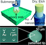
Lipomi, Darren J.; Martinez, Ramses V.; Kats, Mikhail A.; Kang, Sung Hoon; Kim, Philseok; Aizenberg, Joanna; Capasso, Federico; Whitesides, George M.
Patterning the Tips of Optical Fibers with Metallic Nanostructures Using Nanoskiving Journal Article
In: Nano Letters, vol. 11, pp. 632–636, 2011.
@article{Lipomi2010,

title = {Patterning the Tips of Optical Fibers with Metallic Nanostructures Using Nanoskiving},

author = {Darren J. Lipomi and Ramses V. Martinez and Mikhail A. Kats and Sung Hoon Kang and Philseok Kim and Joanna Aizenberg and Federico Capasso and George M. Whitesides},

url = {http://pubs.acs.org/doi/abs/10.1021/nl103730g},

year  = {2011},

date = {2011-01-04},

journal = {Nano Letters},

volume = {11},

pages = {632–636},

abstract = {Convenient and inexpensive methods to pattern the facets of optical fibers with metallic nanostructures would enable many applications. This communication reports a method to generate and transfer arrays of metallic nanostructures to the cleaved facets of optical fibers. The process relies on nanoskiving, in which an ultramicrotome, equipped with a diamond knife, sections epoxy nanostructures coated with thin metallic films and embedded in a block of epoxy. Sectioning produces arrays of nanostructures embedded in thin epoxy slabs, which can be transferred manually to the tips of optical fibers at a rate of approximately 2 min−1, with 88% yield. Etching the epoxy matrices leaves arrays of nanostructures supported directly by the facets of the optical fibers. Examples of structures transferred include gold crescents, rings, high-aspect-ratio concentric cylinders, and gratings of parallel nanowires.},

keywords = {},

pubstate = {published},

tppubtype = {article}

}
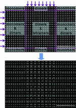
Kang, Sung Hoon; Pokroy, Boaz; Mahadevan, L.; Aizenberg, Joanna
Control of Shape and Size of Nanopillar Assembly by Adhesion-Mediated Elastocapillary Interaction Journal Article
In: ACS Nano, vol. 4, pp. 6323–6331, 2010, (Featured on the cover and highlighted in the issue.).
@article{Kang2010,

title = {Control of Shape and Size of Nanopillar Assembly by Adhesion-Mediated Elastocapillary Interaction},

author = {Sung Hoon Kang and Boaz Pokroy and L. Mahadevan and Joanna Aizenberg},

url = {http://pubs.acs.org/doi/abs/10.1021/nn102260t},

year  = {2010},

date = {2010-11-01},

journal = {ACS Nano},

volume = {4},

pages = {6323–6331},

abstract = {Control of self-organization of nanofibers into regular clusters upon evaporation-induced assembly is receiving increasing attention due to the potential importance of this process in a range of applications including particle trapping, adhesives, and structural color. Here we present a comprehensive study of this phenomenon using a periodic array of polymeric nanopillars with tunable parameters as a model system to study how geometry, mechanical properties, as well as surface properties influence capillary-induced self-organization. In particular, we show that varying the parameters of the building blocks of self-assembly provides us with a simple means of controlling the size, chirality, and anisotropy of complex structures. We observe that chiral assemblies can be generated within a narrow window for each parameter even in the absence of chiral building blocks or a chiral environment. Furthermore, introducing anisotropy in the building blocks provides a way to control both the chirality and the size of the assembly. While capillary-induced self-assembly has been studied and modeled as a quasi-static process involving the competition between only capillary and elastic forces, our results unequivocally show that both adhesion and kinetics are equally important in determining the final assembly. Our findings provide insight into how multiple parameters work together in capillary-induced self-assembly and provide us with a diverse set of options for fabricating a variety of nanostructures by self-assembly.},

note = {Featured on the cover and highlighted in the issue.},

keywords = {},

pubstate = {published},

tppubtype = {article}

}
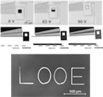
Leblanc, Valerie; Chen, Jianglong; Kang, Sung Hoon; Bulovic, Vladimir; Schmidt, Martin A.
Micromachined Printheads for the Evaporative Patterning of Organic Materials and Metals Journal Article
In: Journal of Microelectromechanical Systems, vol. 16, pp. 394 – 400 , 2007.
@article{Leblanc2007,

title = {Micromachined Printheads for the Evaporative Patterning of Organic Materials and Metals },

author = {Valerie Leblanc and Jianglong Chen and Sung Hoon Kang and Vladimir Bulovic and Martin A. Schmidt},

url = {http://ieeexplore.ieee.org/xpl/login.jsp?tp=&arnumber=4147590&url=http%3A%2F%2Fieeexplore.ieee.org%2Fiel5%2F84%2F4147571%2F04147590.pdf%3Farnumber%3D4147590},

year  = {2007},

date = {2007-04-10},

journal = {Journal of Microelectromechanical Systems},

volume = {16},

pages = {394 - 400 },

abstract = {This paper describes the design, fabrication, and testing of electrostatically actuated microshutters used as active shadow masks to pattern evaporated materials. The fabricated microshutters can obstruct a 25-mum-wide aperture at an actuation voltage of 90 V, with a resonant frequency of 4 kHz due to a 400-mum-long actuator. The microshutters integrated with an x-y-z manipulator were used to print patterns of organic material and metal on glass substrates in vacuum with a pixel size of 25 mum. The maximum resolution achievable with this setup is 800 dpi, and we printed active organic light-emitting device arrays of 400 dpi resolution. This printing scheme could enable the patterning of large-area organic optoelectronic devices on diverse substrates.},

keywords = {},

pubstate = {published},

tppubtype = {article}

}
Note: Send e-mail to Prof. Kang at shkang@jhu.edu if you need a pdf file of the papers below.
2016

Kang, Sung Hoon; Michael D. Dickey, Guest Editors
Patterning via self-organization and self-folding: Beyond conventional lithography Journal Article
In: MRS Bulletin, vol. 41, no. 2, pp. 93-96, 2016, (co-Guest Editor of the issue).
Abstract | Links | BibTeX | Tags: Patterning, Self-Folding, Self-Organization
@article{Kang2016,

title = {Patterning via self-organization and self-folding: Beyond conventional lithography },

author = {Sung Hoon Kang and Michael D. Dickey, Guest Editors},

editor = {Sung Hoon Kang and Michael D. Dickey},

url = {http://journals.cambridge.org/download.php?file=%2FMRS%2FMRS41_02%2FS0883769416000038a.pdf&code=ffd6509119daa4a591802b67ab63f032},

doi = {10.1557/mrs.2016.3 },

year  = {2016},

date = {2016-02-01},

journal = {MRS Bulletin},

volume = {41},

number = {2},

pages = {93-96},

abstract = {Conventional photolithography is an effective patterning technique that has enabled modern

electronics and advanced micro- and nanoscale devices. However, it has limitations, including

high cost, limited resolution, and poor compatibility with unconventional materials that may be

soft, nonplanar, or difficult to process. There is active research ongoing to develop unconventional

patterning methods such as self-organization and self-folding. Self-organization harnesses

various driving forces to produce patterns without external intervention and includes

methods such as self-assembly of block copolymers, capillary-driven assembly of micro-/

nanoscale structures, and thin-fi lm instabilities. Self-folding (origami)—and its cousin,

kirigami—harnesses patterning and materials strategies to convert planar substrates into

three-dimensional shapes in response to external stimuli. These multidisciplinary approaches

open many engineering opportunities by providing new and versatile material functionalities.

This article overviews the field and the topics covered in the articles in this issue of  MRS Bulletin, highlighting recent progress in patterning approaches based on self-organization and self-folding. },

note = {co-Guest Editor of the issue},

keywords = {Patterning, Self-Folding, Self-Organization},

pubstate = {published},

tppubtype = {article}

}
electronics and advanced micro- and nanoscale devices. However, it has limitations, including
high cost, limited resolution, and poor compatibility with unconventional materials that may be
soft, nonplanar, or difficult to process. There is active research ongoing to develop unconventional
patterning methods such as self-organization and self-folding. Self-organization harnesses
various driving forces to produce patterns without external intervention and includes
methods such as self-assembly of block copolymers, capillary-driven assembly of micro-/
nanoscale structures, and thin-fi lm instabilities. Self-folding (origami)—and its cousin,
kirigami—harnesses patterning and materials strategies to convert planar substrates into
three-dimensional shapes in response to external stimuli. These multidisciplinary approaches
open many engineering opportunities by providing new and versatile material functionalities.
This article overviews the field and the topics covered in the articles in this issue of MRS Bulletin, highlighting recent progress in patterning approaches based on self-organization and self-folding.
2011
Seminara, Agnese; Pokroy, Boaz; Kang, Sung Hoon; Brenner, Michael P.; Aizenberg, Joanna
On the Mechanism of Nanostructure Movement under Electron Beam and Its Application in Patterning Journal Article
In: Physical Review B, vol. 83, pp. 235438, 2011.
Abstract | Links | BibTeX | Tags: Actuation, Electron Beam, Electrostatic, Nanopillar, Patterning
@article{Seminara2011,

title = {On the Mechanism of Nanostructure Movement under Electron Beam and Its Application in Patterning},

author = {Agnese Seminara and Boaz Pokroy and Sung Hoon Kang and Michael P. Brenner and Joanna Aizenberg},

url = {http://journals.aps.org/prb/abstract/10.1103/PhysRevB.83.235438},

year  = {2011},

date = {2011-06-30},

journal = {Physical Review B},

volume = {83},

pages = {235438},

abstract = {In electron microscopy, the motion of the sample features due to the interaction with the electron beam has been traditionally regarded as a detrimental effect. Uncontrolled feature displacement produces artifacts both in imaging and patterning, limiting the resolution and distorting precise nanoscale patterns. The mechanism of such motion remains largely unclear. We present an experimental study of e-beam-induced nanopost movement and offer a mechanistic theoretical model that quantitatively explains the physical phenomenon. We propose that e-beam bombardment produces an uneven distribution of electrons in the sample, and the resulting electrostatic interactions provide forces and torques sufficient to bend the nanoposts. We compare the theoretical predictions with a series of controlled experiments that support our model. We take advantage of this theoretical understanding to demonstrate how this generally undesirable effect can be turned into an unconventional e-beam writing technique to generate pseudo-three-dimensional structures.},

keywords = {Actuation, Electron Beam, Electrostatic, Nanopillar, Patterning},

pubstate = {published},

tppubtype = {article}

}
Lipomi, Darren J.; Martinez, Ramses V.; Kats, Mikhail A.; Kang, Sung Hoon; Kim, Philseok; Aizenberg, Joanna; Capasso, Federico; Whitesides, George M.
Patterning the Tips of Optical Fibers with Metallic Nanostructures Using Nanoskiving Journal Article
In: Nano Letters, vol. 11, pp. 632–636, 2011.
Abstract | Links | BibTeX | Tags: Metallic, Nanoskiving, Nanostructure, Optical Fiber, Patterning
@article{Lipomi2010,

title = {Patterning the Tips of Optical Fibers with Metallic Nanostructures Using Nanoskiving},

author = {Darren J. Lipomi and Ramses V. Martinez and Mikhail A. Kats and Sung Hoon Kang and Philseok Kim and Joanna Aizenberg and Federico Capasso and George M. Whitesides},

url = {http://pubs.acs.org/doi/abs/10.1021/nl103730g},

year  = {2011},

date = {2011-01-04},

journal = {Nano Letters},

volume = {11},

pages = {632–636},

abstract = {Convenient and inexpensive methods to pattern the facets of optical fibers with metallic nanostructures would enable many applications. This communication reports a method to generate and transfer arrays of metallic nanostructures to the cleaved facets of optical fibers. The process relies on nanoskiving, in which an ultramicrotome, equipped with a diamond knife, sections epoxy nanostructures coated with thin metallic films and embedded in a block of epoxy. Sectioning produces arrays of nanostructures embedded in thin epoxy slabs, which can be transferred manually to the tips of optical fibers at a rate of approximately 2 min−1, with 88% yield. Etching the epoxy matrices leaves arrays of nanostructures supported directly by the facets of the optical fibers. Examples of structures transferred include gold crescents, rings, high-aspect-ratio concentric cylinders, and gratings of parallel nanowires.},

keywords = {Metallic, Nanoskiving, Nanostructure, Optical Fiber, Patterning},

pubstate = {published},

tppubtype = {article}

}
2010
Kang, Sung Hoon; Pokroy, Boaz; Mahadevan, L.; Aizenberg, Joanna
Control of Shape and Size of Nanopillar Assembly by Adhesion-Mediated Elastocapillary Interaction Journal Article
In: ACS Nano, vol. 4, pp. 6323–6331, 2010, (Featured on the cover and highlighted in the issue.).
Abstract | Links | BibTeX | Tags: Adhesion, bio-inspired science and engineering, Elastocapillary, Evaporation, Nanopillar, Patterning, Self-Organization
@article{Kang2010,

title = {Control of Shape and Size of Nanopillar Assembly by Adhesion-Mediated Elastocapillary Interaction},

author = {Sung Hoon Kang and Boaz Pokroy and L. Mahadevan and Joanna Aizenberg},

url = {http://pubs.acs.org/doi/abs/10.1021/nn102260t},

year  = {2010},

date = {2010-11-01},

journal = {ACS Nano},

volume = {4},

pages = {6323–6331},

abstract = {Control of self-organization of nanofibers into regular clusters upon evaporation-induced assembly is receiving increasing attention due to the potential importance of this process in a range of applications including particle trapping, adhesives, and structural color. Here we present a comprehensive study of this phenomenon using a periodic array of polymeric nanopillars with tunable parameters as a model system to study how geometry, mechanical properties, as well as surface properties influence capillary-induced self-organization. In particular, we show that varying the parameters of the building blocks of self-assembly provides us with a simple means of controlling the size, chirality, and anisotropy of complex structures. We observe that chiral assemblies can be generated within a narrow window for each parameter even in the absence of chiral building blocks or a chiral environment. Furthermore, introducing anisotropy in the building blocks provides a way to control both the chirality and the size of the assembly. While capillary-induced self-assembly has been studied and modeled as a quasi-static process involving the competition between only capillary and elastic forces, our results unequivocally show that both adhesion and kinetics are equally important in determining the final assembly. Our findings provide insight into how multiple parameters work together in capillary-induced self-assembly and provide us with a diverse set of options for fabricating a variety of nanostructures by self-assembly.},

note = {Featured on the cover and highlighted in the issue.},

keywords = {Adhesion, bio-inspired science and engineering, Elastocapillary, Evaporation, Nanopillar, Patterning, Self-Organization},

pubstate = {published},

tppubtype = {article}

}
2007
Leblanc, Valerie; Chen, Jianglong; Kang, Sung Hoon; Bulovic, Vladimir; Schmidt, Martin A.
Micromachined Printheads for the Evaporative Patterning of Organic Materials and Metals Journal Article
In: Journal of Microelectromechanical Systems, vol. 16, pp. 394 – 400 , 2007.
Abstract | Links | BibTeX | Tags: Evaporation, Fabrication, Metal, Organic, Patterning, Printing
@article{Leblanc2007,

title = {Micromachined Printheads for the Evaporative Patterning of Organic Materials and Metals },

author = {Valerie Leblanc and Jianglong Chen and Sung Hoon Kang and Vladimir Bulovic and Martin A. Schmidt},

url = {http://ieeexplore.ieee.org/xpl/login.jsp?tp=&arnumber=4147590&url=http%3A%2F%2Fieeexplore.ieee.org%2Fiel5%2F84%2F4147571%2F04147590.pdf%3Farnumber%3D4147590},

year  = {2007},

date = {2007-04-10},

journal = {Journal of Microelectromechanical Systems},

volume = {16},

pages = {394 - 400 },

abstract = {This paper describes the design, fabrication, and testing of electrostatically actuated microshutters used as active shadow masks to pattern evaporated materials. The fabricated microshutters can obstruct a 25-mum-wide aperture at an actuation voltage of 90 V, with a resonant frequency of 4 kHz due to a 400-mum-long actuator. The microshutters integrated with an x-y-z manipulator were used to print patterns of organic material and metal on glass substrates in vacuum with a pixel size of 25 mum. The maximum resolution achievable with this setup is 800 dpi, and we printed active organic light-emitting device arrays of 400 dpi resolution. This printing scheme could enable the patterning of large-area organic optoelectronic devices on diverse substrates.},

keywords = {Evaporation, Fabrication, Metal, Organic, Patterning, Printing},

pubstate = {published},

tppubtype = {article}

}